Panel Level Packaging Market Growth, Trends, and Strategic Insights
The global panel level packaging market is experiencing rapid growth as semiconductor manufacturers increasingly adopt advanced packaging technologies to meet rising performance demands in high-speed computing, artificial intelligence, automotive electronics, and next-generation communication systems. Panel level packaging is emerging as a highly efficient alternative to wafer-level packaging by enabling larger substrate formats, improved throughput, and lower packaging costs for complex semiconductor assemblies.
The increasing complexity of semiconductor architecture, rapid expansion of heterogeneous integration, and rising demand for compact, high-performance chips are key factors accelerating market development. Manufacturers are focusing on high-density interconnects, enhanced thermal performance, and advanced packaging structures that support faster data transfer, improved miniaturization, and greater manufacturing efficiency.
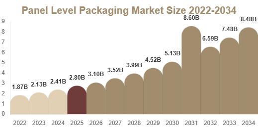
Market Size 2025 – USD 2.8 Billion
Market Size 2034 – USD 8.6 Billion | CAGR – 13.4%
Get Your Sample Report Here: https://packagingmarketinsights.com/report/panel-level-packaging-market/request-sample
Buy Now Full Report: https://packagingmarketinsights.com/buy-now/panel-level-packaging-market
Market Size Link: https://packagingmarketinsights.com/report/panel-level-packaging-market
Market Drivers
Rising Demand for Advanced Semiconductor Packaging
The growing need for smaller, faster, and more powerful semiconductor devices is driving adoption of panel level packaging. This technology supports higher input/output density, improved electrical performance, and better package integration for modern chip designs.
Expansion of Artificial Intelligence and High-Performance Computing
AI processors, data center accelerators, and high-performance computing chips require advanced packaging architectures that offer superior signal integrity and thermal management. Panel level packaging is increasingly being used to meet these demanding requirements.
Growth in Heterogeneous Integration Technologies
The semiconductor industry is rapidly shifting toward heterogeneous integration, where multiple chips with different functions are combined into one package. Panel level packaging enables scalable and cost-effective manufacturing for these advanced integrated systems.
Cost Efficiency and Manufacturing Scale
Compared with wafer-level packaging, panel-level processes allow larger substrate utilization and improved production economics. This supports greater manufacturing output while lowering packaging costs per unit.
Strong Demand from Automotive Electronics
The increasing use of advanced driver assistance systems, electric vehicle electronics, and automotive computing modules is creating new demand for reliable advanced semiconductor packaging technologies.
Market Challenges
High Initial Capital Investment
Panel level packaging requires advanced manufacturing equipment, process development, and facility upgrades, creating substantial capital expenditure requirements for packaging manufacturers.
Process Complexity
Precision alignment, material compatibility, and thermal management challenges can affect production yields, making process optimization critical for commercial-scale manufacturing.
Limited Standardization Across the Industry
The market continues to face challenges related to panel size standards, equipment compatibility, and process integration, which can slow broad industry adoption.
Supply Chain Dependency
Advanced semiconductor packaging depends heavily on specialized materials, substrate technologies, and precision equipment, making the supply chain highly complex and sensitive to disruptions.
Market Segmentation
By Packaging Type
The market includes fan-out panel level packaging, embedded die packaging, and advanced substrate-based panel packaging. Fan-out panel level packaging holds a major market share due to its ability to deliver high-density interconnect performance and compact package designs.
By Material Type
Organic substrates dominate the market because of cost efficiency and compatibility with high-volume manufacturing. Glass substrates are gaining interest for improved dimensional stability, while advanced polymer materials are supporting next-generation packaging designs.
By Application
Applications include AI processors, graphics processing units, memory devices, networking chips, automotive semiconductors, RF components, and IoT devices. AI chips and high-performance computing processors represent strong growth segments due to advanced packaging requirements.
By End-Use Industry
Major end-use sectors include consumer electronics, automotive electronics, telecommunications, industrial automation, healthcare electronics, and data center infrastructure. Telecommunications and AI computing remain major drivers of advanced packaging demand.
By Region
Asia-Pacific dominates the market due to strong semiconductor manufacturing ecosystems in Taiwan, South Korea, China, and Japan. North America remains a major innovation hub driven by advanced chip development and packaging investments. Europe is expanding steadily through automotive semiconductor demand and advanced electronics manufacturing.
Top Players Analysis
- TSMC
TSMC is a leading semiconductor foundry advancing panel-level and next-generation advanced packaging technologies for AI chips, high-performance processors, and integrated semiconductor systems. - Samsung Electronics
Samsung continues expanding advanced semiconductor packaging capabilities with strong investments in heterogeneous integration and high-density packaging innovation. - ASE Technology Holding
ASE is a major outsourced semiconductor assembly and test provider with advanced packaging solutions supporting high-performance computing and next-generation chip integration. - Intel Corporation
Intel is investing heavily in advanced semiconductor packaging architectures, including high-density integration technologies designed for AI and data center applications. - Amkor Technology
Amkor is a global leader in semiconductor packaging services with strong expertise in advanced packaging platforms and integrated package solutions. - JCET Group
JCET is expanding its advanced packaging portfolio with focus on high-density semiconductor packaging and scalable manufacturing technologies. - Powertech Technology Inc.
Powertech supports advanced semiconductor assembly solutions, particularly in memory packaging and high-performance semiconductor packaging systems. - Deca Technologies
Deca Technologies is recognized for innovative advanced packaging approaches focused on cost efficiency, miniaturization, and scalable semiconductor integration. - Nepes Corporation
Nepes develops advanced packaging solutions for semiconductor manufacturers with growing involvement in next-generation integration technologies. - AT&S
AT&S supplies advanced substrates and packaging technologies that support high-performance semiconductor package development worldwide.
Market Outlook
The panel level packaging market is expected to witness strong long-term expansion through 2034, supported by rising AI chip demand, next-generation computing systems, automotive electronics growth, and the increasing complexity of semiconductor integration. Continuous innovation in packaging materials, manufacturing precision, and substrate engineering will remain central to market competitiveness.