Semiconductor Metrology and Inspection Market Size, Analysis, Trends & Forecast Report, 2033 | UnivDatos
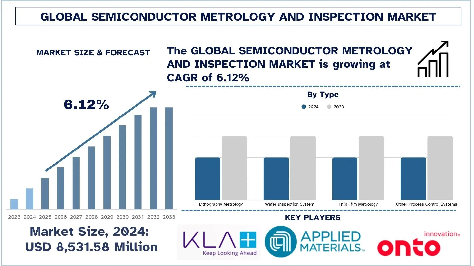
According to a new report by UnivDatos, the Semiconductor Metrology and Inspection Market is expected to reach USD million in 2033 by growing at a CAGR of 6.12% during the forecast period (2025- 2033F). The existing Semiconductor Metrology and Inspection market has a high growth rate due to an ever-increasing number of requirements for smaller, more powerful, and more efficient chips in sophisticated electronics, AI, and automotive markets. With nodes at or below 5nm, it becomes increasingly important to have accuracy in the detection of defects and the accuracy of the process. The need for reliable metrology and inspection products is related to the enhancement of the yield and control of the processes that have to be performed within the semiconductor fabrication cycle, starting with the sequence of inspection actions that establish patterns over the surface of the wafer and ending with the packaging of the semiconductor devices. Advanced alternatives to plasma inspection include optical metrology, advanced X-ray inspection, and e-beam inspection, which is gaining popularity as they have a high resolution capacity. On the other hand, additional advanced inspection equipment is needed with the increase in EUV lithography progression, 3D chip structures, and heterogeneous integration.
Access sample report (including graphs, charts, and figures): https://univdatos.com/reports/semiconductor-metrology-and-inspection-market?popup=report-enquiry
Segments that transform the industry
- The Semiconductor Metrology and Inspection market is segmented into Lithography Metrology, Wafer Inspection Systems, Thin Film Metrology, and Other Process Control Systems. In 2024, the Wafer Inspection System segment dominated the market and is anticipated to continue its leadership throughout the forecast period. With the move of semiconductor nodes to 5nm or less, process validation and accuracy in identifying the defects are critical to process optimization. Wafer inspection systems, through technologies such as e-beam and optical inspection, can perform surface and sub-surface defect inspection in high resolutions over front-end and back-end processes. These systems enable quick detection of the anomalies, thus providing higher reliability of the chips and reducing losses in production. Advanced heterogeneous integration in advanced packaging and the increasing complexity of 3D structures have also driven the demand. Such systems guarantee adherence to strict performance requirements in high-value applications, such as AI processors, automotive silicon, and memory. Driven by the escalating production required by the chip-making industry, the inspection technology serving the wafer industry is emerging as a pivot supporting the key quality, scale, and sustained competitiveness of the chip supply chain globally.
Click here to view the Report Description & TOC https://univdatos.com/reports/semiconductor-metrology-and-inspection-market
According to the report, the impact of the Semiconductor Metrology and Inspection has been identified as high for the North America region. Some of how this impact has been felt include:
North America is now the top-ranked region in Semiconductor Metrology and Inspection and is likely to remain in the top position in the future as well. This leadership has been brought about by a dominance of high-end semiconductor foundries, technology-intensive fab facilities, and a healthy ecosystem of equipment suppliers. The buoyancy of investments in R&D helps the region thrive since recent federal investment in the CHIPS and Science Act has increased domestic semiconductor manufacturing and innovation. The leaders of the US industry are working on state-of-the-art metrology and inspection technologies that can qualify the next generations of module sizes, such as EUV cell and 3D chip designs. The advances in high-performance computing, AI chips, and electric vehicles are driving the industry to higher-performance inspection systems. Furthermore, the presence of leading research and technological companies and organizations ensures a constant stream of innovation and talent. Another future theme is overall chip complexity, which is continuing to increase, and North America specializes in reliability, defect-reduction, and quality-control, thus maintaining its leadership in the market.
Related Report :-
India Semiconductor Market: Current Analysis and Forecast (2024-2032)
EV Semiconductor Market: Current Analysis and Forecast (2022-2030)
Contact Us:
UnivDatos
Contact Number - +1 978 733 0253
Email - contact@univdatos.com
Website - www.univdatos.com
Linkedin- https://www.linkedin.com/company/univ-datos-market-insight/mycompany/