Semiconductor Front-End Equipment Market to Reach USD 175 Billion by 2034 Amid AI Chip and 1nm
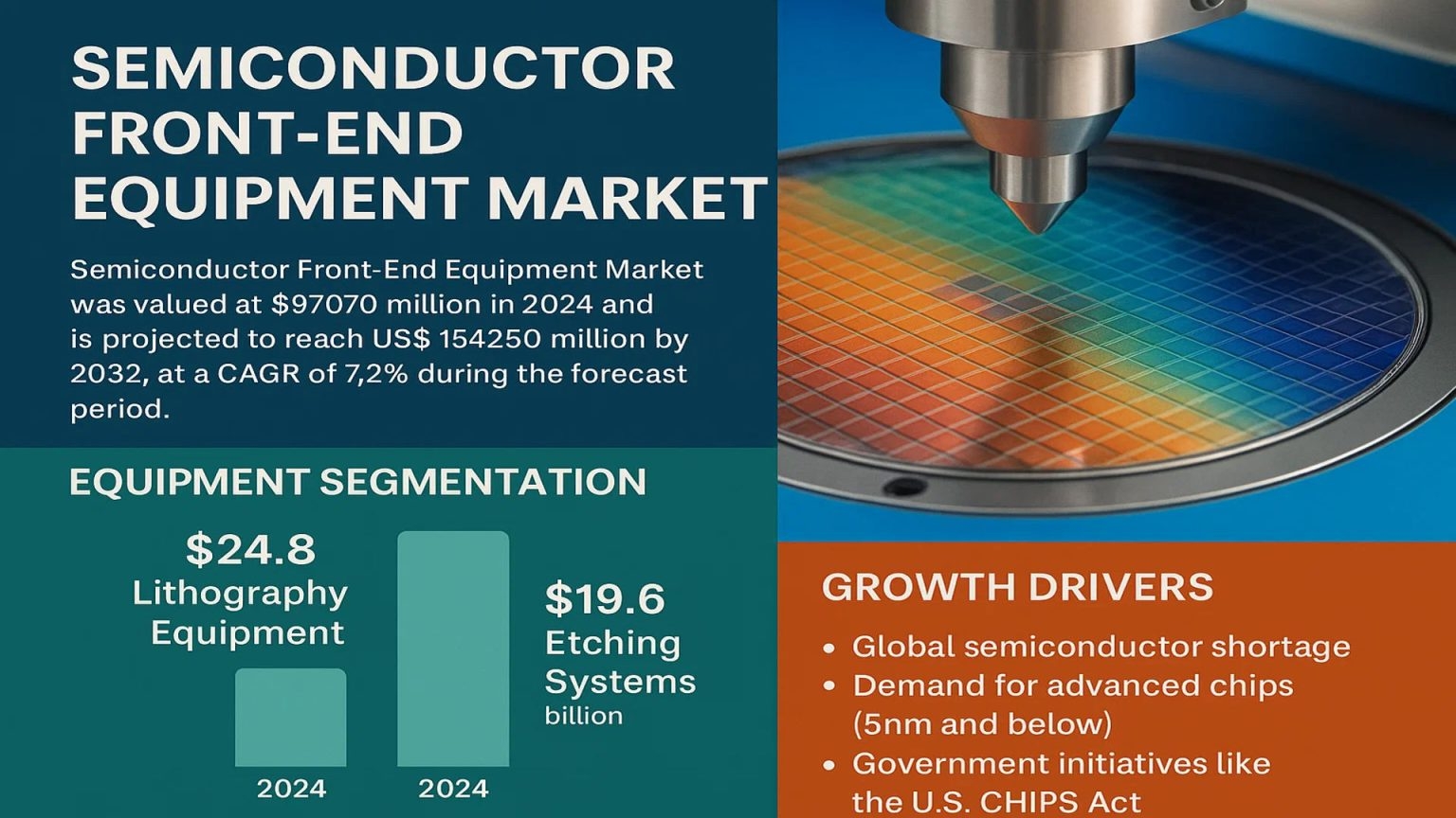
Global Semiconductor Front-End Equipment Market was valued at USD 97,070 million in 2024 and is projected to reach USD 175 billion by 2034, at a CAGR of 6.1% during the forecast period 2026-2034. Massive expansion reflects unprecedented wafer fab construction for A16/1nm logic nodes and HBM4 memory capacity supporting exaflop-scale AI training clusters.
Front-end equipment encompasses EUV/high-NA lithography scanners delivering 8nm pitch resolution, ALD/CVD deposition achieving 2nm nucleation control, and plasma etch systems patterning 100+ layers across 3D NAND decks exceeding 300 active layers. These USD 200M+ EUV tools plus USD 50M etch/deposition clusters enable 300mm wafer throughput exceeding 200k/month per fab, creating 200M+ transistor/cm² densities for TSMC A16, Intel 14A, and Samsung SF2 production ramps.
👉 Access the complete industry analysis and demand forecasts here: https://semiconductorinsight.com/report/semiconductor-front-end-equipment-market/
Market Definition and Dynamics
Semiconductor Front-End Equipment Market supplies capital machinery for wafer processing across 250+ unit operations creating transistor gates, interconnects, and TSV reveal structures, propelled by global cleanroom capacity expanding 20M sqm through 2028 to support 1B+ AI GPUs annually. Core dynamics encompass layer count scaling from 18→35+ EUV exposures per mask set, high-NA 0.55NA scanners doubling chemical consumption per wafer, and backside power delivery networks requiring novel etch/deposition flows.
Process evolution features selective ALD achieving 95% step coverage at 1:50 aspect ratios, cryogenic etch boosting selectivity 5x versus room temperature chemistries, and in-situ metrology enabling 99.5% fab utilization versus legacy 85% baseline.
Market Drivers
- Fab capacity doubling to 25M 300mm-equivalent wafers/month across TSMC/Samsung/Intel three-foundry model for N2P/A16 nodes.
- HBM4 12hi/16hi stack certification consuming 2x front-end processing steps versus HBM3e configurations.
- CHIPS Act/IRA funding triggering USD 450B domestic wafer processing equipment spend through 2030.
- Chiplet ecosystem standardization mandating known-good-die validation across 100+ process flows.
Market Restraints
- EUV light source power scaling capping throughput at 200wph versus 350wph DUV baseline through 2028.
- High-NA EUV pilot tools consuming 2.5x chemical volume with 40% availability versus 85% mature platforms.
- Specialty gas supply constrained to 2 global producers creating single points of failure for 95% fab operations.
Market Opportunities
- Backside power delivery etch/deposition flows for Intel PowerVia/TSMC A16 consuming 25 new unit processes per wafer.
- CFET (Complementary FET) selective deposition requiring atomic layer precision across 200nm pitch.
- 450mm pioneer lines demanding next-gen equipment platforms for Intel PowerVia commercial introduction.
- Domestic EUV scanner qualification under national security mandates shifting 30% global spend patterns.
Competitive Landscape
ASML commands 85% EUV monopoly through High-NA NXE:3400C leadership, Applied Materials/Lam Research/TEL capture 65% etch/deposition volume, while KLA dominates overlay/metrology at 55% share.
List of Key Semiconductor Front-End Equipment Companies
- ASML Holding N.V. (Netherlands)
- Applied Materials, Inc. (U.S.)
- Tokyo Electron Limited (TEL) (Japan)
- NAURA Technology Group (China)
- SEMES (South Korea)
- Hitachi High-Tech (Japan)
- Canon Inc. (Japan)
- Nikon Corporation (Japan)
- Onto Innovation (U.S.)
- Camtek Ltd. (Israel)
- Veeco Instruments (U.S.)
Segment Analysis By Type
Lithography equipment captures 35% revenue leadership through EUV dominance (USD 24.8B in 2024), etching systems follow at 22% (USD 19.6B), while deposition/metrology/cleaning CMP fill remaining capacity across 250+ process steps.
By Application
Foundry/logic drives 60% growth through advanced node ramps, NAND equipment sustains 25% HBM3e/QLC capacity expansion, DRAM provides stable baseline revenue.
Regional Insights
Asia-Pacific dominates 65% capacity via TSMC/Samsung/SMIC 3nm+ lines, North America captures 25% value through Intel/TSMC Arizona fabs, Europe leads specialized equipment (10%), while MEA/South America emerge through regional security mandates.
👉 Access the complete industry analysis and demand forecasts here:
https://semiconductorinsight.com/report/semiconductor-front-end-equipment-market/
📄 Download a free sample to explore segment dynamics and competitive positioning:
https://semiconductorinsight.com/download-sample-report/?product_id=117801
About Semiconductor Insight
Semiconductor Insight is a global intelligence platform delivering data-driven market insights, technology analysis, and competitive intelligence across the semiconductor and advanced electronics ecosystem. Our reports support OEMs, investors, policymakers, and industry leaders in identifying high-growth markets and strategic opportunities shaping the future of electronics.
🌐 https://semiconductorinsight.com
🔗 LinkedIn:Follow Us
📞 International Support: +91 8087 99 2013