Semiconductor Photolithography Equipment Market to Reach USD 36.19 Billion by 2034, Driven by EUV Adoption
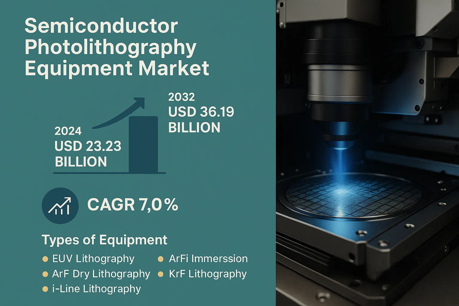
Global Semiconductor Photolithography Equipment Market size was valued at USD 23.23 billion in 2025. The market is projected to grow from USD 24.86 billion in 2026 to USD 36.19 billion by 2034, exhibiting a CAGR of 7.0% during the forecast period (2026-2034). This sustained growth stems from advanced node scaling and global fab investments.
Semiconductor photolithography equipment projects circuit patterns from reticles onto photoresist-coated wafers using coherent light sources, achieving critical dimensions down to 3nm via optical proximity correction and multiple patterning. Systems encompass EUV (13.5nm plasma-generated), ArFi immersion (193nm liquid lens NA=1.35), ArF dry, KrF (248nm), and i-line (365nm) steppers/scanners processing 300mm wafers at 200-300wph throughput with overlay <2nm. Essential in front-end lithography suites for logic/memory at TSMC/Samsung foundries, backend redistribution layers, and photonics waveguides, they demand cleanroom vibration isolation and 250W source power for high-NA EUV.
👉 Access the complete industry analysis and demand forecasts here: https://semiconductorinsight.com/report/semiconductor-photolithography-equipment-market/
Market Definition and Dynamics
The market includes optical/charged-particle exposure tools for wafer patterning in IC fabs, from mask aligners to High-NA EUV scanners priced USD 150-400M/unit. Core forces involve 2nm/1.4nm node ramps consuming 200+ EUV tools/fab and CHIPS Act/equivalent subsidies totaling USD 100B+ for 50 new facilities globally by 2030.
Market Drivers
- AI/HPC chips demand sub-5nm nodes; EUV ships 180+ units in 2024 for 3T+ transistor dies.
- Fab capex hits USD 50B/year; TSMC/Intel expansions order 100 EUV annually.
- 5G/IoT scales memory/logic; ArFi sustains 7-10nm high-volume at 60% market share.
- Geo-diversification funds 20 greenfield fabs; NA/EU incentives boost DUV upgrades.
Market Restraints
- EUV tools cost USD 200M+ with 6-12 month leads; limits to top-5 foundries.
- Supply chain bottleneck on EUV mirrors/lasers; ASML caps 50 units/quarter.
- 90% ASML monopoly raises pricing power amid export controls.
Market Opportunities
- High-NA EUV for 1nm; 0.55NA scanners double density post-2025.
- Advanced packaging lithography; fanout RDL at 2μm pitch for HPC.
- Domestic ArFi/KrF ramps; SMEE serves China 28nm with 30% localization.
Competitive Landscape
ASML commands 90%+ share via EUV monopoly, Nikon/Canon trail in DUV at 10%. SMEE emerges for mature nodes.
Market Dominance by Technological Leaders Drives Intense Competition
List of Key Semiconductor Photolithography Equipment Companies
- ASML Holding N.V.
- Nikon Corporation
- Canon Inc.
- Shanghai Micro Electronics Equipment (SMEE)
Segment Analysis By Type
- EUV Lithography: 40% revenue; essential <7nm, 200W source power.
- ArFi Lithography: High-volume 7-10nm; immersion NA 1.35.
- ArF Dry Lithography: Memory mid-nodes; dry 193nm.
- KrF Lithography: 90-130nm legacy; cost-effective.
- I-line Lithography: Power/analog; 365nm steppers.
By Application
- Front-end Process: 85% share; gate/contact patterning.
- Back-end Process: Packaging RDL/TSV etch.
Regional Insights
Asia-Pacific holds 60% via TSMC/Samsung fabs; North America grows via Intel/CHIPS USD 52B; Europe via ASML ecosystem; China ramps via SMEE amid restrictions.
👉 Access the complete industry analysis and demand forecasts here:
https://semiconductorinsight.com/report/semiconductor-photolithography-equipment-market/
📄 Download a free sample to explore segment dynamics and competitive positioning:
https://semiconductorinsight.com/download-sample-report/?product_id=122777
About Semiconductor Insight
Semiconductor Insight is a global intelligence platform delivering data-driven market insights, technology analysis, and competitive intelligence across the semiconductor and advanced electronics ecosystem. Our reports support OEMs, investors, policymakers, and industry leaders in identifying high-growth markets and strategic opportunities shaping the future of electronics.
🌐 https://semiconductorinsight.com
🔗 LinkedIn:Follow Us
📞 International Support: +91 8087 99 2013