Advanced Process Photomask Market to Reach USD 7.8 Billion by 2034 Driven by EUV Innovation
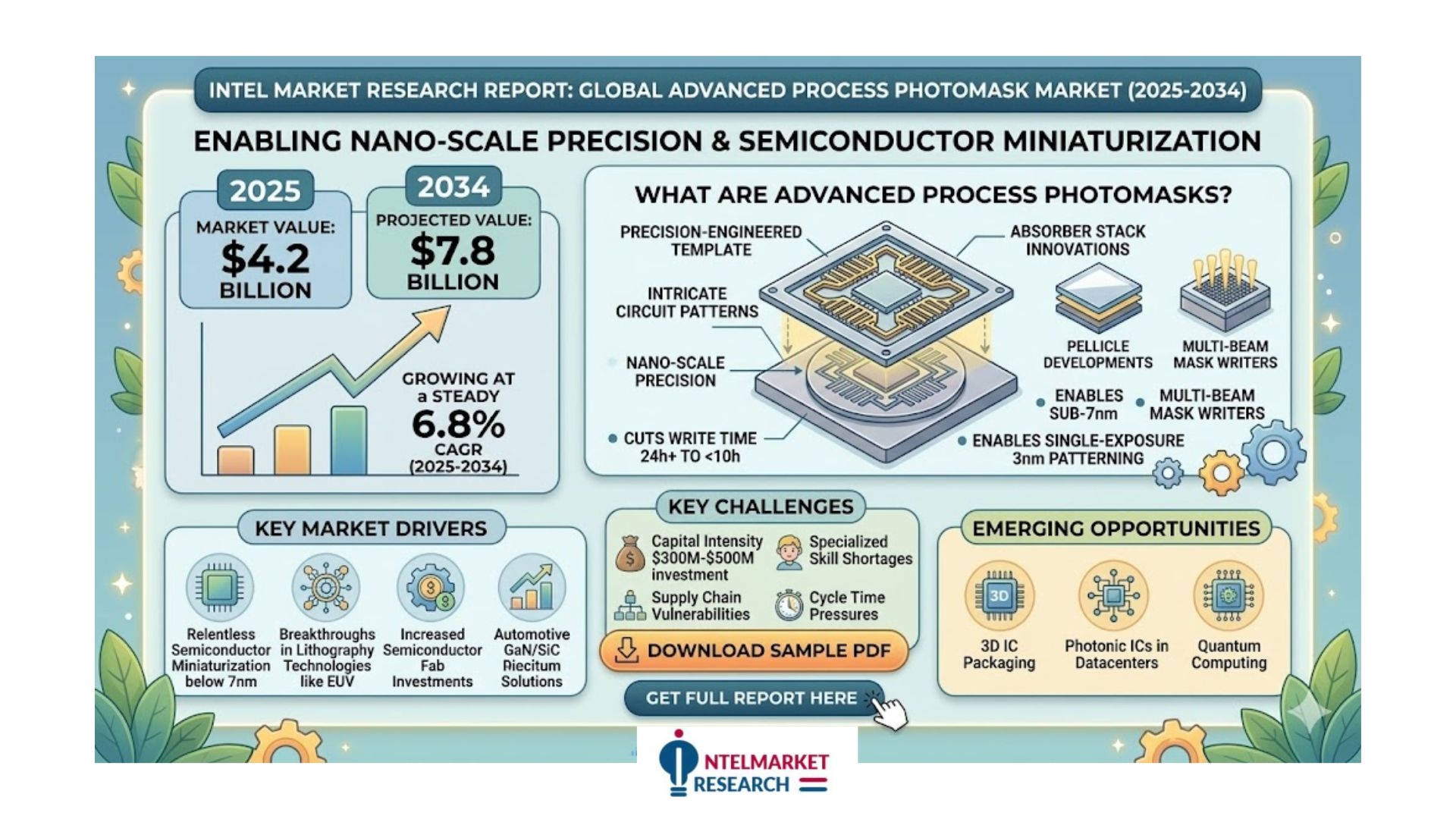
According to a new report from Intel Market Research, the global Advanced Process Photomask market was valued at USD 4.2 billion in 2025 and is projected to reach USD 7.8 billion by 2034, growing at a steady CAGR of 6.8% during the forecast period (2025–2034). This growth is driven by increasing demand for advanced semiconductor nodes, technological advancements in EUV lithography, and rising investments in semiconductor fabrication facilities worldwide.
What are Advanced Process Photomasks?
Advanced Process Photomasks are precision-engineered templates used in semiconductor lithography to transfer intricate circuit patterns onto silicon wafers. These critical components enable the production of cutting-edge chips at nodes like 14nm, 7nm, and below, powering innovations across AI, 5G, and IoT applications. With the semiconductor industry pushing physical limits, photomask technology has become increasingly sophisticated—incorporating phase-shift techniques, multi-beam writing, and specialized materials to achieve nanometer-scale precision.
This comprehensive report provides an authoritative analysis of the Advanced Process Photomask market landscape, covering technological trends, competitive dynamics, regional variations, and detailed segmentations. The insights equip stakeholders across the semiconductor value chain—from foundries and IDMs to equipment suppliers and investors—with strategic intelligence for informed decision-making.
📥 Download Sample Report: Advanced Process Photomask Market - View in Detailed Research Report
Key Market Drivers
1. Accelerating Semiconductor Miniaturization
The relentless push toward smaller process nodes—particularly below 7nm—has dramatically increased photomask complexity. Recent data shows that 7nm masks require 3-4× more write time than 28nm counterparts, while sub-7nm EUV masks demand defect densities below 0.003/cm². This technical arms race is creating sustained demand for high-end photomasks as foundries expand advanced node capacity. With leading players like TSMC allocating over 70% of 2025 capex to 3nm/5nm expansion, the advanced photomask segment is entering a period of accelerated growth.
2. Breakthroughs in Lithography Technologies
The industry's transition to EUV lithography has reshaped photomask requirements, driving adoption of specialized mask architectures:
- Absorber stack innovations - Improved tantalum-based films enable higher EUV absorption with better CD uniformity
- Pellicle developments - Next-gen silicon-based membranes withstand higher power EUV sources while maintaining transmission
- Multi-beam mask writers - Cutting write times from 24+ hours to under 10 hours for complex masks
"The integration of computational lithography with advanced photomasks is enabling single-exposure patterning at 3nm—a $5M+ cost saving per mask set" - Semiconductor Engineering Journal, 2023
These innovations are critical as the industry addresses challenges like stochastic effects and line-edge roughness at atomic scales.
Market Challenges
- Capital Intensity - Establishing an advanced photomask production line requires $300M-$500M in equipment investment, creating significant entry barriers
- Supply Chain Vulnerabilities - Dependence on single-source suppliers for critical materials (ultra-pure quartz, specialized resists) creates bottlenecks
- Talent Shortages - The specialized skill set required for mask data preparation and defect engineering limits production scalability
- Cycle Time Pressures - Maintaining 5-7 day turnaround times for advanced masks while managing increasing complexity
Emerging Opportunities
The Advanced Process Photomask market is evolving beyond traditional semiconductor applications, creating new revenue streams:
- 3D IC Packaging - Fan-out and hybrid bonding technologies require specialized mask solutions for dense interconnects
- Photonic ICs - Silicon photonics adoption in datacenters is driving demand for unique phase-control mask features
- Automotive GaN/SiC - Power electronics manufacturing demands rugged masks capable of handling thicker resist layers
- Quantum Computing - Emerging qubit fabrication processes present novel mask challenges in cryogenic environments
📥 Download Sample PDF: Advanced Process Photomask Market - View in Detailed Research Report
Regional Market Insights
- Asia-Pacific (68% market share) - Dominated by Taiwan's TSMC ecosystem and Korea's memory-focused supply chain. China's domestic mask shops are rapidly advancing capabilities with government support.
- North America (18%) - Concentrated around Intel's IDM model and leading fabless companies. Strong R&D in next-gen patterning and computational lithography.
- Europe (9%) - ASML's EUV leadership drives specialized mask technology development, particularly for high-NA systems.
- Emerging Markets - Israel and Singapore are establishing niche capabilities in specialty applications like MEMS and sensors.
Market Segmentation
By Node Type
- 14nm
- 7nm
- 5nm & Below
- EUV-specific
By Application
- Logic
- Memory (DRAM/NAND)
- Foundry Services
- IDM Production
By End-Use Industry
- Consumer Electronics
- Data Center/Cloud
- Automotive
- Industrial IoT
By Technology
- Optical Lithography
- EUV Lithography
- Nanoimprint
- Directed Self-Assembly
📘 Get Full Report: Advanced Process Photomask Market - View Detailed Research Report
Competitive Landscape
The market is concentrated among three global leaders—Photronics, Toppan, and DNP—who collectively control ~65% of advanced photomask production. However, the landscape is evolving with:
- Foundries developing captive mask shops (TSMC Mask Center, Samsung Mask Team)
- Emerging Chinese players (SMIC Mask, PKU Mask) supported by national semiconductor initiatives
- Equipment makers (Applied Materials, Lasertec) vertically integrating into adjacent process steps
The report provides detailed competitive analysis of 18 key players, evaluating their technology roadmaps, capacity expansions, and strategic partnerships across the semiconductor ecosystem.
Report Deliverables
- Comprehensive market sizing (value/volume) and growth forecasts through 2034
- Technology adoption curves for EUV, multi-patterning, and next-gen lithography
- Cost structure analysis and CAPEX benchmarking
- Supply chain risk assessment and vendor positioning
- Regulatory impacts (export controls, materials restrictions)
- Strategic recommendations for equipment suppliers, material vendors, and foundries
📘 Get Full Report: Advanced Process Photomask Market - View Detailed Research Report
📥 Download Sample Report: Advanced Process Photomask Market - View in Detailed Research Report
About Intel Market Research
Intel Market Research is a leading provider of strategic intelligence, offering actionable insights in semiconductors, advanced manufacturing, and industrial technologies. Our research capabilities include:
- Real-time competitive benchmarking
- Technology adoption lifecycle modeling
- Supply chain risk mapping
- 400+ industrial reports annually
Trusted by Fortune 500 technology firms, our insights empower executives to navigate complex market transitions with confidence.
🌐 Website: https://www.intelmarketresearch.com
📞 Asia-Pacific: +91 9169164321
🔗 LinkedIn: Follow Us