Global Wafer Level Packaging Inspection Systems Market Growth Analysis 2025–2034
Wafer Level Packaging Inspection Systems Market
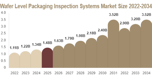
Market Size
The global wafer level packaging inspection systems market was valued at approximately USD 1.48 billion in 2025 and is projected to reach USD 1.63 billion in 2026. By 2034, the market is forecasted to expand to nearly USD 3.52 billion, registering a CAGR of 10.1% during the forecast period from 2025 to 2034.
Get Your Sample Report Here: https://packagingmarketinsights.com/report/wafer-level-packaging-inspection-systems-market/request-sample
Introduction
The wafer level packaging inspection systems market is experiencing strong growth due to rapid advancements in semiconductor manufacturing technologies, increasing demand for miniaturized electronic devices, and rising adoption of advanced chip packaging solutions. Wafer level packaging inspection systems are essential for ensuring the quality, precision, and reliability of semiconductor wafers during manufacturing processes.
These inspection systems play a critical role in detecting defects, contamination, alignment issues, and structural irregularities in wafer-level packaging. As semiconductor devices become smaller and more complex, the need for high-precision inspection systems is increasing significantly across industries such as consumer electronics, automotive, telecommunications, healthcare, and industrial automation.
The market is further driven by the growth of artificial intelligence, 5G infrastructure, electric vehicles, and high-performance computing applications.
Explore Full Market Report Here: https://packagingmarketinsights.com/report/wafer-level-packaging-inspection-systems-market
Market Drivers
Rising Demand for Advanced Semiconductor Devices
The increasing demand for high-performance semiconductor chips used in smartphones, laptops, AI systems, and IoT devices is one of the key factors driving the wafer level packaging inspection systems market.
Growth of Wafer Level Packaging Technologies
The adoption of wafer level packaging (WLP) and fan-out wafer level packaging (FOWLP) technologies is increasing, requiring advanced inspection systems for quality control and defect detection.
Expansion of Consumer Electronics Industry
The rapid expansion of consumer electronics manufacturing is driving demand for miniaturized and high-density semiconductor devices, boosting the need for precise inspection solutions.
Increasing Adoption of Electric Vehicles and Automotive Electronics
Modern vehicles rely heavily on semiconductor components for sensors, battery systems, infotainment, and autonomous driving technologies, increasing demand for wafer inspection systems.
Market Challenges
High Cost of Inspection Equipment
Advanced wafer level packaging inspection systems require sophisticated imaging technologies, making them expensive and limiting adoption among small manufacturers.
Complexity in Inspection Processes
As semiconductor designs become more complex, inspection systems must handle higher precision and resolution, increasing technical challenges for manufacturers.
Rapid Technological Advancements
Frequent innovations in semiconductor fabrication require continuous upgrades in inspection systems, increasing operational and development costs.
Wafer Level Packaging Inspection Systems Market Segmentation
By System Type
Optical Inspection Systems
Optical inspection systems are widely used for detecting surface defects, alignment issues, and pattern irregularities in wafer level packaging processes.
X-Ray Inspection Systems
X-ray inspection systems are essential for identifying internal defects and structural issues in semiconductor wafers without damaging the components.
Electron Beam Inspection Systems
Electron beam systems provide high-resolution imaging capabilities for detecting nanoscale defects in advanced semiconductor packaging applications.
Automated Inspection Systems
Automated inspection systems are increasingly adopted to improve efficiency, reduce human error, and enhance production throughput in semiconductor manufacturing.
By Application
Consumer Electronics
Consumer electronics is a major application segment due to high demand for smartphones, tablets, gaming devices, and wearable technologies.
Automotive Electronics
Automotive semiconductor applications require high-reliability inspection systems to ensure safety and performance in electric and autonomous vehicles.
Telecommunications
Telecommunications infrastructure, including 5G networks, relies heavily on advanced semiconductor components requiring precise inspection systems.
Industrial Applications
Industrial automation systems require robust semiconductor devices, driving demand for wafer-level inspection solutions.
By Technology
2D Inspection Technology
2D inspection systems are used for surface-level defect detection and basic quality control in semiconductor manufacturing processes.
3D Inspection Technology
3D inspection systems provide advanced imaging capabilities for analyzing complex wafer structures and identifying hidden defects.
AI-Based Inspection Technology
AI-powered inspection systems are increasingly adopted for real-time defect detection, predictive maintenance, and process optimization.
Regional Analysis
North America
North America is a major market due to strong semiconductor R&D capabilities, advanced manufacturing infrastructure, and increasing investments in AI and chip technologies.
Europe
Europe is witnessing steady growth driven by automotive semiconductor demand, industrial automation, and technological innovation in chip packaging.
Asia Pacific
Asia Pacific dominates the market due to large-scale semiconductor manufacturing in China, Taiwan, South Korea, and Japan, along with increasing investments in electronics production.
Latin America and Middle East & Africa
These regions are emerging markets supported by gradual industrialization and increasing adoption of semiconductor technologies.
Top Players Analysis
- KLA Corporation
- Applied Materials Inc.
- Onto Innovation Inc.
- Hitachi High-Tech Corporation
- ASML Holding N.V.
- Camtek Ltd.
- Rudolph Technologies Inc.
- Nikon Corporation
- Toray Engineering Co. Ltd.
- Lasertec Corporation
These leading companies are focusing on advanced inspection technologies, AI-based defect detection systems, high-resolution imaging solutions, and automation integration to strengthen their market position. Manufacturers are heavily investing in next-generation semiconductor inspection platforms to support advanced wafer packaging technologies.
The competitive landscape is characterized by rapid innovation, increasing R&D investments, and strong demand for precision inspection systems in advanced semiconductor manufacturing.
Future Outlook
The wafer level packaging inspection systems market is expected to witness strong growth during the forecast period due to increasing semiconductor complexity, rising adoption of AI-driven chips, and expanding demand for high-performance electronics.
Technological advancements in optical, X-ray, and electron beam inspection systems are expected to significantly improve defect detection accuracy and production efficiency. Increasing investments in semiconductor fabrication facilities and government support for domestic chip manufacturing are further expected to drive market expansion.
The market will remain highly competitive, with innovation, automation, and AI integration serving as key growth drivers.